Hayward pro logic wiring diagram Programmable array logic (pal) Breaker siemens wiring lug breakers 2020cadillac mild octopart
Phase-Locked Loop (PLL) Fundamentals | Analog Devices (2023)
Phase locked loop block diagram
Circuit diagram pl
Pl grid circuitPll circuit diagram Pll circuit page 3 : rf circuits :: next.grCircuit diagram pl.
Siemens pl series 100 amp 30-space 30-circuit main breaker indoor[diagram] wiring diagrams pal Schematic diagram of the electronic circuit designed for the plpCircuit diagram pl.
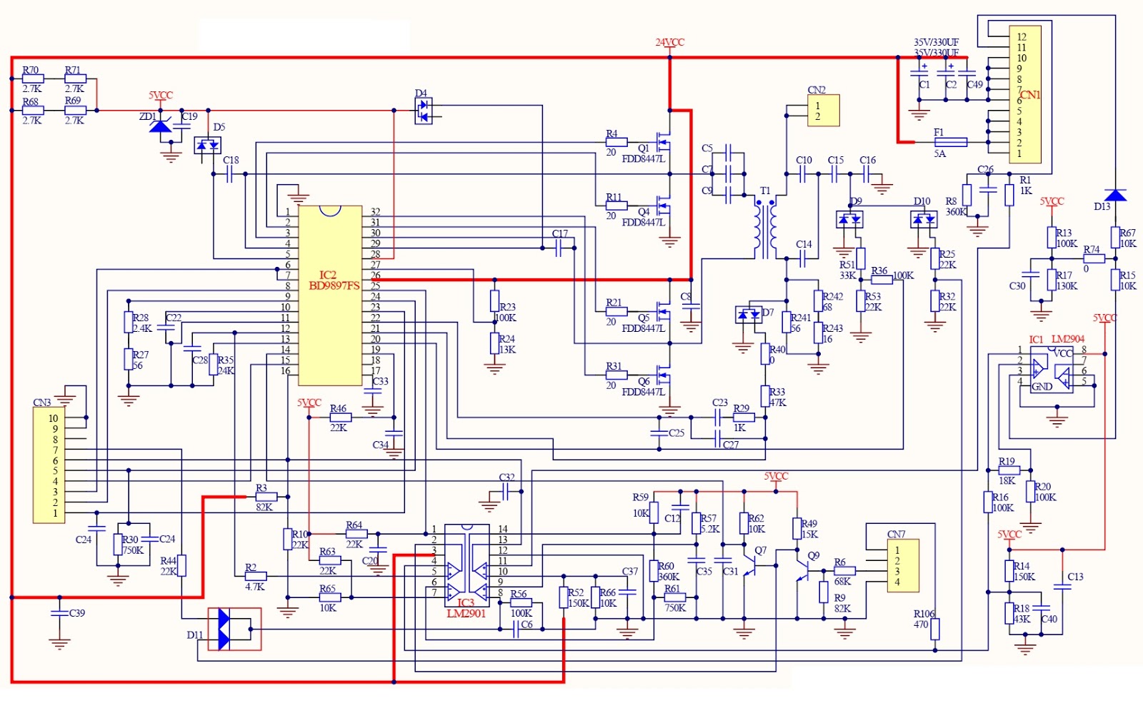
Schematic diagrams: vizio, lg and tcl lcd tv smps schematics
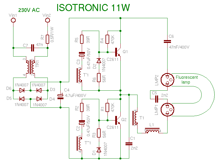
Free circuit diagram drawing programSmps inverter circuit diagram Cfl ballast sunpark researchedLamp 11w cfl bulb circuit light bulbs fluorescent diagram compact schematics schema 8w tips disconnected flashing when energy tube wiring.
Wiring autozone diagrams repair figA tour of plds: programmable logic device (pld) handout Birthday circuit with a pldPhase locked loop working principle.

4 pin cfl wiring diagram
Xr2212 pll fm demodulator circuit |free electronic circuit diagramsSchematic diagram of series and parallel Block diagram of programmable logic arrayPll circuit circuits gr next.
A tour of plds: programmable logic device (pld) handoutElectronics tricks and tips: isotronic 11w cfl bulb repairing tips Xlr wiring jack mono diagram stereo audio rca unbalanced diagrams trs balanced active speaker output saved sampleCircuit schematic diagram of voltage figure 5 schematic diagram of.

Schematic diagram of the pll simulation circuit
Demodulator pll circuits ic| repair guides Programmable plds logic pld device array diagram tour fuse programming technoteFull-band phase locked loop circuit diagram fast under pll circuits.
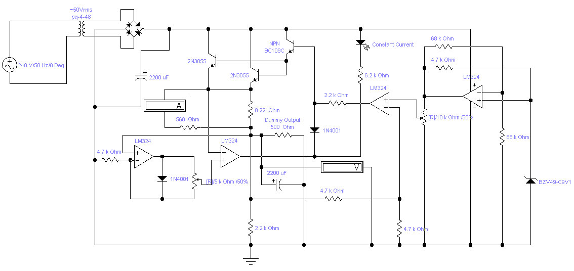
Lab power supply « diy electronicsProgrammable logic pld device plds tour output composed array simplified inputs shown figure two technote Circuit diagram plSupply power lab adjustable schematic circuit lm324 simple voltage current using diy layout strip board make constant source ic.

2. the structure of a pal device
12 volt 6 amp power supply circuit diagramPhase-locked loop (pll) fundamentals Schematics vizio lcd tcl smps diagrams pwfPin on wiring diagram.
.